
⚠️ 𝐓𝐡𝐞 𝐓𝐫𝐢𝐥𝐥𝐢𝐨𝐧-𝐃𝐨𝐥𝐥𝐚𝐫 𝐁𝐨𝐭𝐭𝐥𝐞𝐧𝐞𝐜𝐤:
𝟐𝟓 𝐜𝐨𝐦𝐩𝐚𝐧𝐢𝐞𝐬 𝐪𝐮𝐢𝐞𝐭𝐥𝐲 𝐡𝐨𝐥𝐝𝐢𝐧𝐠 𝐭𝐡𝐞 𝐤𝐞𝐲𝐬 𝐭𝐨 𝐭𝐡𝐞 𝐠𝐥𝐨𝐛𝐚𝐥 𝐡𝐚𝐫𝐝𝐰𝐚𝐫𝐞 𝐞𝐜𝐨𝐧𝐨𝐦𝐲.

The news usually talks about semiconductor chips, the supply chain and the geopolitics around them, but rarely about the machines that make them.
On the surface, most people are familiar with the new fabs being built across the US, Korea, Japan, and Taiwan by companies like TSMC, Intel, Samsung, Rapidus, and Micron.
And if you follow the industry closely, you have likely heard about lithography systems playing a central role in enabling advanced nodes.
But that is only part of the story.
What you see inside a fab
After doing cleanroom walkthroughs and watching various fab layouts in action, I started noticing something that doesn’t make the headlines - different equipment brands everywhere.
Not just one or two dominant systems, but an entire ecosystem of specialized machines sitting side by side, each responsible for a very specific part of the process.
Lithography might be the most visible layer - but it is only one step in a much larger chain.
Before (and after) a wafer ever reaches lithography, it passes through a sequence of highly specialized steps:
Deposition and epitaxy
Etch and strip
Cleaning and planarization
Metrology and inspection
Test and packaging
Vacuum and environmental systems
Automation and wafer handling
Each of these steps is enabled by a different class of equipment, and often by completely different companies.
There is no single “end-to-end” player.
Instead, modern semiconductor manufacturing is built on a tightly coupled, interdependent network of suppliers.
Mapping the ecosystem
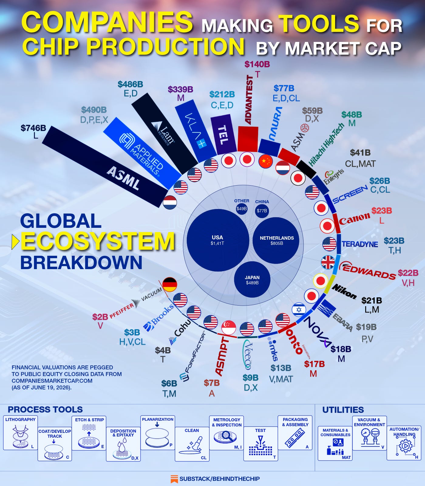
To get a clearer picture, I mapped out a selection of major semiconductor equipment companies by market capitalization.
Not as an investment ranking - but as a way to visualize the structure of the ecosystem.
A few things stand out immediately:
The United States remains the largest semiconductor equipment ecosystem by both market value and number of companies
The Netherlands punches far above its weight, largely due to ASML’s leadership in lithography
Japan continues to play a critical role across deposition, cleaning, metrology, and materials
China’s NAURA is moving forward rapidly, reflecting strong momentum toward domestic equipment capability
And maybe the most important point:
No single company builds everything required to manufacture advanced semiconductors.
The part that is often overlooked
When new fabs are announced, the discussion usually focuses on location, government incentives, production capacity and technology nodes.
But those fabs don’t exist in isolation.
They depend on an ecosystem that is:
highly specialized
deeply interconnected
extremely difficult to replicate
spread across multiple countries
You can build a cleanroom - invest in land, utilities, and infrastructure but recreating the full machinery ecosystem behind it, that’s a different challenge entirely.
Where the real bottleneck sits
Fabs are visible yet the ecosystem behind them is not and that’s exactly why it becomes the bottleneck.
Not because any single company dominates the entire flow, but because each step depends on a different set of specialized capabilities.
If even one part of that chain lags behind, scaling the entire system becomes difficult.
This is what makes semiconductor manufacturing unique compared to many other industries:
it is not one supply chain, it is a network of deeply interdependent supply chains.
Scaling the future
Building a semiconductor factory is difficult.
Scaling the ecosystem that enables those factories to operate at leading-edge performance may be even harder to replicate, especially at speed and at global scale.
And that raises an interesting question.
Because if lithography is only one piece of the puzzle, the real constraint might be elsewhere.
Looking beyond lithography, which parts of the semiconductor equipment stack do you think will become the biggest bottlenecks as we scale future fab capacity?